Table of Contents
ToggleSemiconductor Startup Business : Step by Step Guide
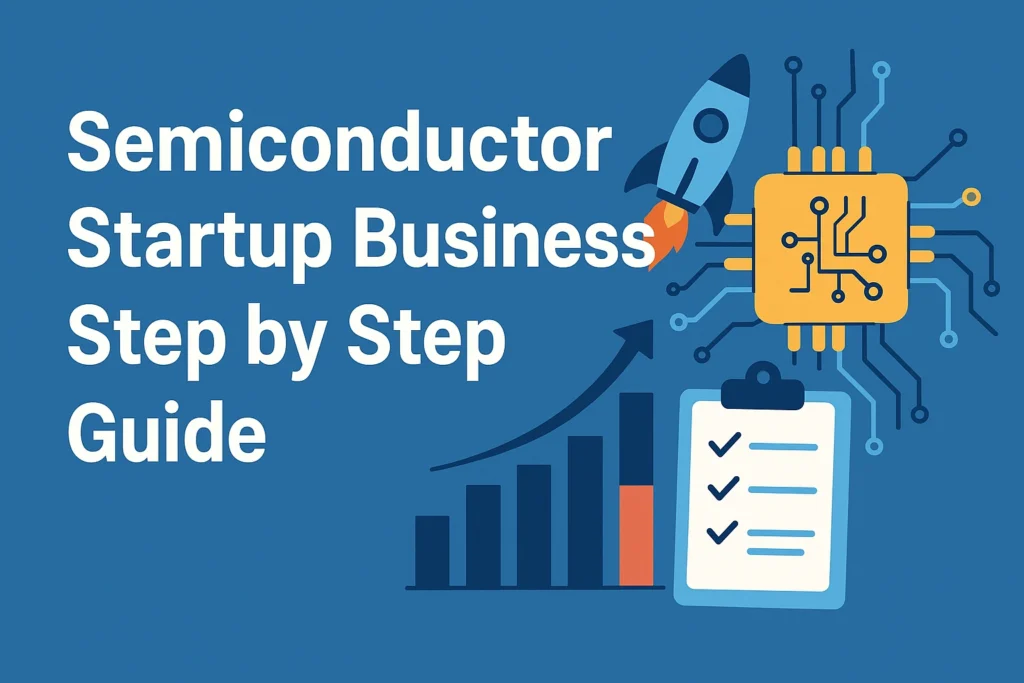
The Semiconductor Startup Journey
A visual guide to navigating the complex but rewarding path of launching a chip company, from initial idea to market success.
An Unprecedented Market Opportunity
The global semiconductor market is experiencing explosive growth, creating fertile ground for innovative startups.
$624B
Projected Global Revenue in 2024
A significant rebound driven by demand in AI and automotive sectors.
> $1T
Projected Market Size by 2030
The industry is on a trajectory to nearly double in size by the end of the decade.
90%
of Startups Choose the Fabless Model
This model minimizes massive upfront capital costs for manufacturing plants.
Market & Business Planning
This initial phase is about laying a solid foundation through strategic research, niche selection, and robust planning.
Identifying High-Growth Niches
Startups must target segments with accelerated demand. Artificial Intelligence and Automotive are leading the charge, requiring highly specialized, powerful, and efficient chips.
Allocating Startup Capital
A fabless startup's initial costs are dominated by talent and specialized software. Securing foundry access for prototyping is a smaller but critical expense.
From Digital Design to Physical Chip
The core of a semiconductor venture is the highly complex journey of transforming a concept into a functional silicon chip through design, fabrication, and testing.
Chip Design
Front-end (RTL) & Back-end (Physical Layout)
Tape-Out
Final design submitted to a foundry.
Foundry Fabrication
Wafers manufactured (e.g., TSMC, GlobalFoundries)
Packaging & Test
Chips are sliced, packaged, and tested by an OSAT partner.
Final Product
A functional, market-ready semiconductor chip.
Productization & Go-To-Market
With a physical product, the focus shifts to sales, marketing, and scaling production for commercial success.
Securing Funding for Growth
Capital is the lifeblood of a semiconductor startup. Government grants and deep-tech Venture Capital are primary sources, with corporate partnerships offering strategic advantages.
Government Grants
Programs like the U.S. CHIPS Act and India's Semicon Program offer significant non-dilutive funding.
Venture Capital
Deep-tech focused VCs provide capital and industry expertise, crucial for scaling.
Corporate Partnerships
Alliances with large tech firms can provide funding, market access, and technical resources.
Effective B2B Sales Channels
Reaching technical buyers requires a multi-channel approach. Direct sales to large OEMs offer deep integration, while distributors provide broader market access and logistics support.
Semiconductor Startup Business Guide: From Idea to Production & Sales
Executive Summary: Charting the Course for Semiconductor Startup Success
The semiconductor industry, a foundational layer of the modern digital economy, is experiencing a transformative period, presenting unprecedented opportunities for agile startups. The strategic advantages of the fabless business model, characterized by reduced capital expenditure and an intense focus on innovation, position it as the optimal entry point for new ventures. This guide delineates a comprehensive, step-by-step pathway for semiconductor startups, spanning initial market planning and legal establishment through intricate chip design, fabrication, production, and ultimately, productization, sales, and sustainable growth. Success in this complex landscape hinges on strategic partnerships, robust intellectual property protection, and the judicious leveraging of available government incentives and industry programs.
Introduction: The Dynamic Landscape of Semiconductor Innovation
The global semiconductor industry stands as a critical enabler of technological progress, underpinning virtually every electronic device and system in use today. This sector is not merely about manufacturing components; it is a complex ecosystem of design, intellectual property (IP) development, specialized materials, equipment manufacturing, and sophisticated production processes. The rapid pace of innovation has led to chips integrating billions of transistors on a single silicon slice, making the world smarter, healthier, and more connected.
The industry's trajectory is marked by significant growth, with global semiconductor revenue projected to rebound strongly, reaching an estimated $624 billion in 2024 and potentially exceeding $1 trillion by the end of the decade. This expansion is fueled by an increasing demand for chips across various high-growth segments, including artificial intelligence (AI), edge computing, automotive electronics, medical devices, and the Internet of Things (IoT). The shift towards silicon-defined vehicles, the rollout of 5G and Wi-Fi 7 networks, and the burgeoning need for AI accelerators are particularly strong drivers.
Despite its immense potential, the semiconductor industry is characterized by high capital intensity, geopolitical complexities, and a persistent talent gap. However, these challenges also create unique opportunities for innovative startups. The emergence of specialized business models and supportive government initiatives, such as the U.S. CHIPS Act and India's Semicon Program, are democratizing access to resources and fostering a more resilient and diversified global supply chain. This environment is ripe for new entrants who can identify niche markets, develop cutting-edge designs, and navigate the intricate path from concept to commercialization.
PHASE 1: MARKET & BUSINESS PLANNING
Step 1: Understanding the Semiconductor Ecosystem and Business Models
A foundational understanding of the semiconductor ecosystem is paramount for any aspiring startup. This intricate landscape comprises various types of chips and distinct business models that define how companies operate within the value chain.
Types of Chips and Their Applications
- Logic Chips: These are the "brains" of electronic devices, performing computational tasks. Examples include Central Processing Units (CPUs), Graphics Processing Units (GPUs), Application-Specific Integrated Circuits (ASICs), and Systems-on-Chips (SoCs). They are critical for AI workloads, high-performance computing (HPC), and complex embedded systems.
- Memory Chips: These store data, either temporarily (DRAM – Dynamic Random-Access Memory) or permanently (NAND flash memory). The memory market is expected to see a robust recovery, with significant growth projected in 2024.
- Analog/Power Chips: These manage and convert power, process real-world signals (like sound or temperature), and are crucial for power management in various applications.
- Specialty Chips: This category includes AI accelerators, Radio Frequency (RF) chips, sensors, and other highly specialized components designed for specific functions or emerging technologies. Demand for AI accelerators, particularly GPU-based servers, is a significant growth driver.
PHASE 1: MARKET & BUSINESS PLANNING
Step 1: Understanding the Semiconductor Ecosystem and Business Models (cont.)
Core Business Models: IDM, Fabless, Foundry, OSAT
The semiconductor industry has evolved into a highly disaggregated structure, with companies specializing in different stages of the production process.
- Integrated Device Manufacturers (IDMs): These companies handle the entire process from chip design to fabrication, assembly, and testing in-house. Intel and Samsung (for certain products) are prime examples. IDMs own and operate their own fabrication plants ("fabs"), which are immensely capital-intensive, costing billions of dollars to build and maintain. While they may also utilize foundries, their core model involves self-sufficiency in manufacturing.
- Fabless Companies: These companies focus exclusively on chip design, research, and marketing, outsourcing the manufacturing process to third-party foundries. NVIDIA, AMD, and Qualcomm are prominent fabless players. This model allows them to concentrate resources on innovation and design, leveraging the economies of scale offered by foundries.
- Foundries: These are companies that specialize solely in the manufacturing of chips for other companies, operating large-scale fabrication plants. TSMC (Taiwan Semiconductor Manufacturing Company) is the undisputed leader in logic chip foundry services, with Samsung and GlobalFoundries also being major players. Building a new generation fab can cost upwards of $20 billion.
- Outsourced Semiconductor Assembly and Test (OSAT) Companies: These providers specialize in the post-fabrication stages, including die slicing (cutting wafers into individual chips), packaging (enclosing the chip in a protective housing), and rigorous testing to ensure quality and reliability. ASE, Amkor, and JCET are leading OSAT providers. OSATs are indispensable for fabless companies and IDMs seeking to outsource overflow or reduce operational expenses, enabling them to streamline production and focus on core competencies.
PHASE 1: MARKET & BUSINESS PLANNING
Step 1: Understanding the Semiconductor Ecosystem and Business Models (cont.)
Strategic Consideration: The Fabless Model as the Optimal Entry Point for Startups
For a semiconductor startup, the fabless model typically represents the most viable and strategic entry point. This approach offers significant advantages by mitigating the astronomical capital costs associated with building and operating a fabrication plant. A state-of-the-art foundry can cost over $20 billion, an investment far beyond the reach of most startups.
By outsourcing manufacturing, fabless companies can significantly decrease initial investment and infrastructure expenses, freeing up capital for other strategic investments like research and development (R&D) and talent acquisition. This model enhances product development agility, allowing startups to respond swiftly to evolving market demands and customer needs. The ability to rapidly prototype and iterate cutting-edge chip designs without manufacturing constraints accelerates innovation. Furthermore, it facilitates collaboration with specialized foundries, granting access to advanced manufacturing techniques that would otherwise be unattainable. This flexibility and focus on core competencies—design, innovation, and marketing—are crucial for sustaining a competitive advantage in the dynamic semiconductor industry.
| Business Model | Pros for Startups (Fabless Focus) | Cons for Startups (Fabless Focus) |
|---|---|---|
| Fabless | - Lower capital investment (no fabs) - Focus on core design and innovation - Enhanced agility and faster time-to-market - Access to advanced foundry technologies - Reduced overhead costs | - Reliance on third-party foundries for manufacturing capacity and technology - Potential for supply chain vulnerabilities - Less control over manufacturing process and yield optimization |
| IDM | - Full control over design and manufacturing - Potential for optimized integration | - Extremely high capital expenditure (billions for a fab) - Significant operational complexity and overhead - Slower adaptation to market shifts due to fixed assets |
| Foundry | Not a typical startup entry model | - Requires massive capital investment in fabs - Focus on manufacturing processes, not chip design - High R&D costs for process technology |
| OSAT | Not a typical startup entry model | - Requires specialized assembly and testing facilities - Focus on packaging and testing, not chip design |
PHASE 1: MARKET & BUSINESS PLANNING
Step 2: Strategic Market Research and Niche Identification
Effective market research is the cornerstone of a successful semiconductor startup, enabling the identification of underserved niches and high-growth opportunities.
Identifying Market Gaps and High-Growth Segments
The semiconductor market is vast, but certain segments are experiencing accelerated demand and innovation, making them attractive for new ventures. Key areas include:
- AI Chips: Artificial intelligence and high-performance computing (HPC) are major drivers of semiconductor demand, requiring advanced chips with exceptional computational power and energy efficiency. The generative AI chip market alone is projected to exceed $150 billion in 2025, with the total addressable market for AI accelerator chips potentially reaching $500 billion by 2028. This demand extends to workload accelerators for data centers, supporting both training and inference of AI workloads.
- Edge Computing: With the rise of IoT applications, there is a strong demand for chips that excel in processing data closer to the source, reducing latency and bandwidth requirements.
- Automotive: The automotive industry is undergoing a significant transformation from mechanical to silicon-defined vehicles, driven by autonomous driving, enhanced connectivity, and advanced sensors. This shift mandates cutting-edge semiconductor technologies, with 3nm nodes now entering the automotive sector. Functional safety standards like ISO 26262 are critical for chips in this domain.
- Medical Devices: Semiconductors are increasingly vital for advanced medical applications, including diagnostics, imaging, and implantable devices.
- IoT (Internet of Things): The proliferation of connected devices across consumer electronics, industrial automation, and smart infrastructure fuels demand for specialized, energy-efficient chips.
PHASE 1: MARKET & BUSINESS PLANNING
Step 2: Strategic Market Research and Niche Identification (cont.)
Leveraging Industry Reports and Market Intelligence
To pinpoint these opportunities, startups should leverage authoritative industry reports and market intelligence. Organizations like Gartner, McKinsey, and the Semiconductor Industry Association (SIA) provide invaluable data and analysis.
- Gartner: Offers detailed semiconductor revenue forecasts, market trend analyses, and supply chain insights, including inventory levels and technology roadmaps. Their reports highlight shifts away from high-volume, high-content market drivers and the increasing importance of semiconductors as a national security issue.
- McKinsey: Provides insights into market capitalization, supply chain vulnerabilities, and investment trends within the semiconductor industry. Their analyses indicate significant investments in U.S. semiconductor manufacturing capacity and potential supply gaps for critical materials.
- Semiconductor Industry Association (SIA): Represents the U.S. semiconductor industry and provides comprehensive market data, policy agendas, and reports on global sales trends, R&D programs, and workforce challenges. SIA reports project substantial growth in U.S. domestic semiconductor manufacturing capacity and a leading share in advanced logic manufacturing by 2032.
Defining Your Target Customer and Problem-Solution Fit
Beyond identifying broad market trends, a startup must precisely define its target customer and the specific problem it aims to solve. This involves understanding customer pain points, existing solutions, and how the proposed chip offering provides a superior value proposition. The most successful ventures quantify the customer value in tangible business terms, such as cost savings or performance improvements, rather than solely technical specifications. This clear problem-solution fit is essential for attracting both customers and investors.
PHASE 1: MARKET & BUSINESS PLANNING
Step 2: Strategic Market Research and Niche Identification (cont.)
| Market Segment | Key Growth Drivers & Applications | Relevant Chip Types |
|---|---|---|
| AI & HPC | Generative AI, Large Language Models, Data Centers, Cloud Computing, Edge AI | AI Accelerators, GPUs, High-Bandwidth Memory (HBM), ASICs, specialized SoCs |
| Automotive | Autonomous Driving, Advanced Driver-Assistance Systems (ADAS), Electric Vehicles (EVs), Connectivity, Infotainment | Image Sensors, Radars, Lidars, Vision Processors, AI Chips, Power Management ICs, 3nm nodes |
| IoT | Smart Homes, Industrial IoT, Wearables, Connected Devices, Edge Computing | Low-power SoCs, Sensors, Connectivity Chips (Wi-Fi 7, 5G), Microcontrollers |
| Telecommunications | 5G Networks, Wi-Fi 7, Data Centers, High-Speed Data Transfer | RF Chips, Integrated Photonics, High-Speed Transceivers |
| Medical Devices | Diagnostics, Imaging, Implantables, Wearable Health Monitors | Sensors, Low-power Processors, Analog Front-Ends |
PHASE 1: MARKET & BUSINESS PLANNING
Step 3: Developing a Robust Business Plan
A well-structured business plan serves as the blueprint for a semiconductor startup, articulating its vision, strategy, and financial projections. This document is crucial for internal alignment and for securing external funding.
Defining Problem, Solution, Target Market, and Product Offering
The business plan must clearly define the problem the startup is addressing and the unique solution its chip offers. This includes specifying the type of chip (e.g., a custom ASIC, a specialized SoC) and its intended application or target customer. The product offering should highlight how it provides superior value compared to existing solutions, emphasizing competitive advantages such as patents, trade secrets, or unique performance characteristics.
Crafting Your Go-to-Market and Revenue Models
A clear go-to-market strategy is essential, outlining how the chip will reach its target customers. This involves identifying sales channels (e.g., direct to Original Equipment Manufacturers (OEMs), through distributors), marketing initiatives, and customer rollout plans. The revenue model must detail how the company will generate income, whether through direct sales, licensing, or services, and should be structured to attract investors by demonstrating a clear path to profitability.
PHASE 1: MARKET & BUSINESS PLANNING
Step 3: Developing a Robust Business Plan (cont.)
Estimating Critical Costs: EDA Tools, IP Licensing, Fabrication, and Personnel
Semiconductor startups face substantial upfront and ongoing costs. A detailed cost estimation is vital for financial planning and funding requests.
- Design Software (EDA Tools): Electronic Design Automation (EDA) tools are indispensable for chip design, simulation, and verification. Leading EDA suites from companies like Cadence, Synopsys, and Mentor Graphics (Siemens EDA) are highly sophisticated and expensive. Professional tool licenses can cost between $100,000 to $200,000 per year per seat. While open-source alternatives like OpenROAD exist, they may not suffice for tape-out-ready designs. Some EDA providers offer startup programs or special pricing.
- Licensing IP Blocks: Modern chip designs frequently incorporate pre-designed intellectual property (IP) blocks for common functions like USB, PCIe, DDR memory controllers, or processor cores (e.g., ARM, RISC-V). Licensing these blocks reduces design cycles, lowers verification effort, and mitigates functional bugs. ARM's standard Flexible Access package can cost around $200,000 annually, with additional license and royalty fees. Open-source RISC-V cores can be free to use, though commercial RISC-V IP providers may charge license fees, often without royalties.
- Fabrication (Foundry Access): The cost of manufacturing chips is a major expenditure. Multi-Project Wafer (MPW) services, or shuttle runs, allow multiple designs to share a single wafer, significantly reducing initial fabrication costs for prototyping and testing. For example, a 28nm chip using Europractice (an MPW service) can cost around €10,700 per mm², with a minimum area requirement. Full mask runs for production volumes are substantially more expensive.
- Personnel: A skilled team of chip designers, verification engineers, and other specialists is crucial. Salaries for senior design engineers can range from $100,000 to $500,000 per year each, with additional costs for software and testing staff or consultants.
PHASE 1: MARKET & BUSINESS PLANNING
Step 3: Developing a Robust Business Plan (cont.)
| Cost Category | Estimated Range / Details | Implications for Startups |
|---|---|---|
| EDA Tool Licenses | $100K - $200K per year per seat for professional tools (Cadence, Synopsys). Open-source options (OpenROAD) are free but may have limitations. Startup programs exist. | Significant recurring operational cost. Leveraging startup programs or open-source tools can reduce initial burden but may require careful evaluation of capabilities for tape-out. |
| IP Core Licensing | ARM: ~$200K annual access fee, plus license & unit royalties upon production. Imagination: $0 license fee, but $135K/year for 2 years of support, royalties upon production. RISC-V: Open-source cores are free; commercial RISC-V IP may have license fees but often no royalties. | Variable costs depending on IP choice. Open-source RISC-V offers cost savings and customization but may have less proven track record or support than proprietary IP. |
| Chip Fabrication (MPW) | ~$12K per square millimeter for TSMC 65nm via Europractice. GlobalFoundries 28nm via Europractice: €10,700 per mm² (min 9mm²). Initial shuttle run: ~$25K. | MPW services are crucial for cost-effective prototyping and initial testing, enabling rapid iteration and bug identification before full production. |
| Full Mask Run | ~$250K for first full mask run (with potential bugs). | Substantial cost for production-ready designs; highlights the importance of thorough verification before tape-out. |
| Personnel (Annual) | 3-5 senior design engineers: $100K - $500K each. Misc. software and testing staff/consultants: ~$500K. Field Application Engineer (FAE): ~$100K. | High personnel costs necessitate efficient team building and clear project milestones to manage burn rate. Experienced talent is critical for complex chip design. |
| Other Costs | Bring-up boards, test equipment, engineering time: ~$100K. Outsourced layout: ~$100K - $200K. Marketing and distribution, physical inventory: Variable. | These costs add to the overall financial burden and require careful budgeting. Outsourcing non-core activities can optimize resource allocation. |
PHASE 1: MARKET & BUSINESS PLANNING
Step 4: Legal Foundations and IP Protection
Establishing a solid legal framework and robust intellectual property (IP) protection is non-negotiable for a semiconductor startup.
Company Incorporation and Legal Setup
The first legal step involves registering the company. A Limited Liability Company (LLC) is a common choice for startups. For startups in India, entities like Private Limited Companies, Limited Liability Partnerships (LLPs), or Partnership Firms are eligible for government schemes, provided they meet criteria such as being less than 10 years old and having an annual turnover under ₹100 crore. The registration process involves submitting identity and address proofs, a business plan, financial statements, and incorporation documents to the relevant authorities.
Securing Intellectual Property (Patents, Design Rights, NDAs)
IP is the lifeblood of a semiconductor company. Protecting proprietary designs, processes, and technologies is critical for maintaining a competitive edge, attracting investors, and preventing reverse engineering.
- Patents: Patents protect unique chip architectures, layouts, and innovative fabrication processes. In India, patents are typically valid for 20 years from the filing date, provided renewal fees are paid. Startups in India can benefit from faster patent registration and a 50% reduction in normal charges under government schemes. Strategic patent filing is crucial, covering system-level patents for integrated circuits that incorporate multiple components, as well as advancements in efficiency, size, and production methods. Active enforcement of patent rights is necessary to prevent unauthorized use.
- Design Rights: These protect the visual appearance of a product or its parts, which can be critical for unique chip packaging or layout elements.
- Non-Disclosure Agreements (NDAs) and Contracts: Establishing comprehensive NDAs with employees, contractors, and vendors is essential to safeguard confidential information and trade secrets. Clear contracts for vendors and employees define relationships, responsibilities, and IP ownership.
PHASE 1: MARKET & BUSINESS PLANNING
Step 4: Legal Foundations and IP Protection (cont.)
Strategic Location Considerations and Incentives
Choosing the right location can significantly impact a semiconductor startup's success. Many countries and regions offer incentives to attract semiconductor businesses due to the industry's strategic importance. These incentives can include grants, tax rebates, and infrastructure support. For instance, the U.S. CHIPS Act and India's Semicon Program offer substantial fiscal support and R&D programs to foster domestic semiconductor ecosystems. Proximity to suppliers, talent pools, stable energy supply, and transport facilities are also critical considerations for site selection, especially for any future manufacturing expansion.
PHASE 2: CHIP DESIGN & DEVELOPMENT
Step 5: Building Your Expert Team
The success of a semiconductor startup hinges on the caliber and synergy of its technical team. Chip design is a highly specialized field requiring diverse expertise.
Essential Roles and Responsibilities in Chip Design
Building a multidisciplinary team with deep domain knowledge is paramount. Key roles typically include:
- Hardware Architects: Responsible for defining the overall chip architecture and specifications, translating product requirements into a high-level design. They make critical power, performance, and area (PPA) trade-offs early in the design cycle.
- RTL Designers (Verilog/VHDL): These engineers translate the architectural specifications into Register Transfer Level (RTL) code using Hardware Description Languages (HDLs) like Verilog or VHDL. They focus on the data flow and control flow of the circuit.
- Verification Engineers: A critical role, verification engineers ensure the chip design functions correctly and meets all specifications before manufacturing. They develop testbenches, verification plans, and use methodologies like Universal Verification Methodology (UVM) to identify and prevent costly errors and defects that could arise during production.
- Physical Design (Back-end) Engineers: These specialists convert the logical RTL design into a physical layout that can be manufactured. Their tasks include synthesis, placement, clock tree synthesis (CTS), routing, and timing closure. They also perform Design Rule Check (DRC) and Layout vs. Schematic (LVS) checks to ensure manufacturability and logical correctness. An experienced backend engineer may take 3-4 months to take a design from Verilog to a foundry-ready file.
- Product Manager: This role bridges the technical and business aspects, defining the product roadmap, understanding market needs, and coordinating between engineering, marketing, and sales teams.
- Software/Firmware Developers (Optional but Recommended): For chips requiring embedded software or firmware, these developers ensure seamless integration and functionality, especially for complex Systems-on-Chips (SoCs).
PHASE 2: CHIP DESIGN & DEVELOPMENT
Step 5: Building Your Expert Team (cont.)
| Role | Key Responsibilities | Importance for Startup Success |
|---|---|---|
| Hardware Architect | Defines chip architecture, specifications, and high-level design; makes PPA (Power, Performance, Area) trade-offs. | Establishes the fundamental blueprint for the chip, directly impacting its capabilities, efficiency, and market fit. |
| RTL Designer | Translates architectural specifications into Register Transfer Level (RTL) code using Verilog/VHDL; implements data flow and control logic. | Creates the core digital logic of the chip, a critical step in translating concept into a functional design. |
| Verification Engineer | Develops testbenches and verification plans; performs functional simulation and testing to ensure design correctness and adherence to specifications. | Prevents costly errors and re-spins post-fabrication, ensuring product quality and accelerating time-to-market. |
| Physical Design Engineer | Converts RTL design into a physical layout; performs synthesis, placement, routing, clock tree synthesis (CTS), timing closure, DRC/LVS checks. | Optimizes the chip's physical implementation for performance, power, and area, making it manufacturable. |
| Product Manager | Defines product roadmap, gathers market requirements, coordinates between engineering, marketing, and sales teams. | Ensures the chip design aligns with market needs and business objectives, guiding product development from conception to launch. |
| Software/Firmware Developer | Develops embedded software/firmware for the chip; ensures hardware-software co-design and integration (optional but often essential). | Critical for enabling chip functionality and delivering a complete solution, especially for SoCs with significant software components. |
PHASE 2: CHIP DESIGN & DEVELOPMENT
Step 6: Selecting Essential Design Tools and IP Blocks
The choice of Electronic Design Automation (EDA) tools and intellectual property (IP) blocks profoundly influences a startup's design capabilities, efficiency, and cost structure.
Choosing Electronic Design Automation (EDA) Tools
EDA tools are specialized software, and sometimes hardware, that assist in the definition, planning, design, implementation, verification, and manufacturing preparation of semiconductor devices. The three primary companies leading the EDA market are Synopsys, Cadence, and Mentor Graphics (now Siemens EDA). These tools are essential for managing the immense complexity of modern chip designs, which can contain billions of circuit elements.
- Cost and Access: Professional-grade EDA tool licenses are a significant investment, often costing $100,000 to $200,000 per year per seat. However, many EDA vendors offer startup programs or collaborate with tech incubators to provide access to their tools at reduced costs or even without equity requirements. For example, Synopsys has partnered with Plug and Play to offer design tool access to selected startups, aiming to lower the barrier to entry. Open-source EDA flows, such as OpenROAD, also exist, offering a free and scalable option for early design exploration, though their suitability for final tape-out may vary.
- Functionality: EDA tools cover various stages, including simulation (modeling circuit behavior), design (assembling circuit elements), and verification (checking logical and physical correctness). Integrated platforms from leading vendors offer comprehensive solutions for front-end and back-end design, verification, and silicon lifecycle management.
PHASE 2: CHIP DESIGN & DEVELOPMENT
Step 6: Selecting Essential Design Tools and IP Blocks (cont.)
Acquiring and Licensing IP Blocks
IP blocks are pre-designed, silicon-proven modules that can be integrated into a chip design, significantly shortening design cycles, reducing verification effort, and lowering the risk of functional bugs.
- ARM: A dominant provider of processor IP, ARM licenses its architecture and cores widely. Access to ARM IP, support, tools, and training can cost around $200,000 annually, with additional license fees and unit-based royalties upon production.
- Imagination Technologies: Offers graphics and AI IP. Their "Open Access" program provides access to IP with no upfront license costs, requiring only a two-year support and maintenance package (e.g., $135,000 per year) and unit royalties once a product ships. This model aims to reduce upfront capital costs for scale-up companies.
- RISC-V: An open-source Instruction Set Architecture (ISA) that has gained significant popularity due to its flexibility and royalty-free nature. While open-source RISC-V cores are free to use, commercial IP providers offer value-added RISC-V cores that may require a license fee, but typically no royalties per chip produced. RISC-V allows designers to customize processors for specific power, performance, and area (PPA) optimizations across a wide range of applications, from IoT devices to high-performance computing. The open-standard nature fosters collaboration and innovation, and its transparency allows for close scrutiny, enhancing security.
PHASE 2: CHIP DESIGN & DEVELOPMENT
Step 6: Selecting Essential Design Tools and IP Blocks (cont.)
Understanding Foundry Process Nodes
The "process node" (e.g., 28nm, 16nm, 7nm, 5nm) refers to a generation of semiconductor manufacturing technology. These terms are primarily marketing labels rather than direct physical measurements of transistor features. Each new node typically signifies increased transistor density (miniaturization), improved speed, and reduced power consumption compared to its predecessor.
- Evolution and Cost: Moving to smaller nodes (e.g., from 28nm to 5nm) involves increasingly complex and expensive fabrication processes, such as Extreme Ultraviolet (EUV) lithography. While leading-edge nodes (like 5nm) offer superior performance and density, they come with higher R&D and mask costs.
- Strategic Choice: Startups must choose a process node that balances their performance requirements, power budget, cost constraints, and target market. Older, more mature nodes (e.g., 28nm) might be more cost-effective for certain applications and have higher available capacity. Newer nodes (e.g., 5nm) are critical for high-performance applications like AI accelerators and advanced CPUs. TSMC's 5nm process (N5) offered 1.8x the density of its 7nm (N7) process, with 15% speed improvement or 30% lower power consumption.
PHASE 2: CHIP DESIGN & DEVELOPMENT
Step 7: Front-End Chip Design: Architecture to RTL
The chip design process is typically divided into "front-end" and "back-end" stages, which are highly interdependent. Front-end design focuses on the functional and logical aspects of the chip.
Specification, Architecture Definition, and PPA Trade-offs
Every ASIC design begins with a clear understanding of the chip's functional requirements and constraints. This involves defining the problem, the solution, and the target application. Based on these, the hardware architecture is planned, breaking down the chip into functional blocks (e.g., CPU, memory, I/O ports, sensor input buffering, compression engines).
During this phase, critical Power, Performance, and Area (PPA) trade-offs are made.
- Performance: How fast the chip operates, typically measured in clock frequency or throughput.
- Power: The energy consumed, including dynamic power (from switching activity) and static power (from leakage currents). Techniques like clock gating, power gating, and multi-voltage domains are employed to manage power consumption.
- Area: The physical silicon space occupied, which directly impacts manufacturing cost and yield.
These parameters are tightly linked, and optimizing one often impacts the others, requiring careful balancing based on the target application.
PHASE 2: CHIP DESIGN & DEVELOPMENT
Step 7: Front-End Chip Design: Architecture to RTL (cont.)
RTL Coding and Functional Verification
Once the architecture is defined, the design is translated into Register Transfer Level (RTL) code using Hardware Description Languages (HDLs) like Verilog or VHDL. RTL describes the circuit's data flow and control flow.
Following RTL coding, extensive functional simulation and verification are performed. This crucial step ensures that the design behaves as intended before committing to the costly physical implementation and fabrication. Verification engineers create testbenches and use various methodologies to thoroughly validate the design, preventing errors that could lead to expensive post-production fixes. A robust verification process is critical to safeguarding the integrity of the final product.
PHASE 2: CHIP DESIGN & DEVELOPMENT
Step 8: Back-End Physical Design and Optimization
The back-end, or physical design, phase transforms the verified RTL design into a manufacturable layout on silicon. This stage is highly complex and involves meticulous optimization to meet PPA targets.
Synthesis, Placement, Clock Tree Synthesis (CTS), and Routing
- Synthesis: The RTL code is translated into a gate-level netlist, which is a representation of the design using standard logic gates (e.g., AND, OR, flip-flops).
- Placement: The logic gates and IP blocks are arranged on the silicon die in an optimal manner to minimize area, reduce wire lengths, and improve performance. Efficient placement is crucial for subsequent steps.
- Clock Tree Synthesis (CTS): A critical step that builds a balanced clock distribution network across the chip. A well-designed clock tree ensures that the clock signal arrives at all sequential elements (like flip-flops) at precisely the same time, preventing timing violations and ensuring reliable operation.
- Routing: After placement, all the placed cells are interconnected using metal wires across multiple layers of the chip. Modern chips can utilize 6-15 metal layers for routing, depending on their complexity. Routing also involves placing vias, which are tiny vertical connections between different metal layers. Proper routing minimizes signal delays, crosstalk, and power consumption.
PHASE 2: CHIP DESIGN & DEVELOPMENT
Step 8: Back-End Physical Design and Optimization (cont.)
Timing Closure and Physical Verification (DRC/LVS)
- Timing Closure: This iterative process ensures that all timing requirements (e.g., clock frequency, setup and hold times) are met across the entire chip. It involves analyzing signal propagation delays and adjusting placement and routing to eliminate timing violations. Achieving timing closure is a significant challenge in high-performance designs.
- Design Rule Check (DRC): Once the physical layout is complete, DRC tools verify that the design adheres to all manufacturing rules specified by the foundry. These rules dictate minimum spacing between wires, minimum wire widths, and other geometric constraints necessary for successful fabrication.
- Layout vs. Schematic (LVS) Checks: LVS tools compare the physical layout with the original logical schematic (netlist) to ensure that no connections were missed, misrouted, or inadvertently added. This check confirms that the physical design accurately reflects the intended logical circuit. Both DRC and LVS are essential for ensuring the design is ready for fabrication and will function as intended.
PHASE 2: CHIP DESIGN & DEVELOPMENT
Step 9: Preparing for Tape-out
Tape-out marks a pivotal moment in the chip development lifecycle: the finalization of the design for submission to a foundry for fabrication.
Finalizing the Design to Send to a Foundry
Before tape-out, the design undergoes exhaustive final checks to ensure it is completely error-free and compliant with the chosen foundry's process design kit (PDK). This includes comprehensive physical verification (DRC, LVS, antenna rule checks, etc.), power integrity analysis (IR drop, electromigration), and signal integrity analysis. Any remaining issues must be resolved to avoid costly re-spins, as manufacturing a chip is extremely expensive. The design data, typically in GDSII format, is then prepared and packaged for transmission to the foundry.
PHASE 2: CHIP DESIGN & DEVELOPMENT
Step 9: Preparing for Tape-out (cont.)
Utilizing Multi-Project Wafer (MPW) Services for Cost Efficiency
For startups, committing to a full production run is a massive financial undertaking. Multi-Project Wafer (MPW) services, also known as shuttle runs, offer a cost-effective solution for prototyping, testing, and validating initial designs.
- Mechanism: MPW services allow multiple chip designs from different companies or research institutions to share space on a single silicon wafer. This dramatically reduces the per-design fabrication cost, as the mask and wafer costs are distributed among several participants.
- Providers: Reputable MPW service providers include MOSIS, Efabless, Europractice, and direct TSMC shuttle runs. For instance, Europractice lists 2022 prices for GlobalFoundries 28nm at €10,700 per mm², with a minimum area. An initial shuttle run can cost around $25,000.
- Benefits: MPW services enable rapid iteration and testing of designs, allowing startups to identify and fix bugs early in the development cycle before investing in a full mask set. This iterative approach is crucial for optimizing performance, power, and area, and for de-risking the design before scaling to mass production. While MPW costs are significantly lower, they are typically for smaller quantities of chips, suitable for validation and sampling rather than high-volume production.
PHASE 3: FABRICATION & PRODUCTION
Step 10: Partnering with a Semiconductor Foundry
Once the chip design is finalized and taped out, the next critical step is to partner with a semiconductor foundry for physical fabrication.
Selecting the Right Fabrication Partner
Choosing a foundry is a strategic decision that impacts cost, performance, and supply chain resilience. Key considerations include:
- Process Node Availability: The foundry must support the chosen process node (e.g., 28nm, 16nm, 7nm, 5nm) and offer the specific technology features required for the chip. Leading foundries continuously invest billions in advancing process nodes.
- Cost and Volume: Foundries offer different pricing structures based on process node, wafer size, and production volume. For startups transitioning from MPW, negotiating favorable terms for larger volumes is crucial.
- Technology Leadership and Reliability: Foundries like TSMC are dominant due to their advanced process technology and ability to mass-produce chips at lower costs and higher yields. They are the backbone for major fabless companies like Apple, AMD, NVIDIA, and Qualcomm.
- Major Foundries: TSMC (global leader), UMC, GlobalFoundries, and SMIC are key players.
PHASE 3: FABRICATION & PRODUCTION
Step 10: Partnering with a Semiconductor Foundry (cont.)
Negotiating Wafer Supply Agreements (WSAs)
A Wafer Supply Agreement (WSA) is a formal contract between the fabless company and the foundry, outlining the terms and conditions for wafer fabrication. These agreements specify pricing, volume commitments, delivery schedules, quality standards, and intellectual property rights. Securing long-term manufacturing agreements with leading foundries is essential for a fabless company's success, ensuring consistent supply and access to advanced technologies. The geopolitical landscape and supply chain vulnerabilities necessitate careful consideration of foundry location and diversification strategies.
| Foundry | Type | Key Offerings / Noteworthy Points |
|---|---|---|
| TSMC | Pure-play | Global leader in logic foundry services; known for cutting-edge nodes (e.g., 5nm, 4nm, 3nm); backbone for major fabless companies like Apple, AMD, NVIDIA, Qualcomm; offers MPW services. |
| Samsung Semiconductor | IDM (also offers foundry services) | Second largest logic foundry; also designs and manufactures its own ICs; strong in memory and advanced logic. |
| GlobalFoundries | Pure-play | Significant pure-play foundry with fabs in the US; offers a range of process nodes, including 22nm FD-SOI. |
| UMC | Pure-play | Major pure-play foundry from Taiwan; offers a variety of process technologies. |
| SMIC | Pure-play | Leading pure-play foundry based in China. |
PHASE 3: FABRICATION & PRODUCTION
Step 11: Post-Fabrication: Packaging & Testing (OSAT)
After wafers are fabricated by a foundry, they are sent to an Outsourced Semiconductor Assembly and Test (OSAT) provider for the crucial final stages of production.
Engaging with OSAT Providers
OSAT companies specialize in transforming bare silicon dies into fully functional, packaged semiconductor components ready for integration into electronic devices. They are indispensable partners for fabless companies, eliminating the need for them to invest heavily in their own assembly and testing facilities. This outsourcing allows fabless firms to scale production flexibly based on market demand and benefit from the OSATs' economies of scale. OSATs also enable front-end fabs to maximize their output by taking over the time-consuming post-fabrication processes.
PHASE 3: FABRICATION & PRODUCTION
Step 11: Post-Fabrication: Packaging & Testing (OSAT) (cont.)
Key OSAT Services: Die Slicing, Packaging, Final Test, and Burn-in
OSAT providers offer a comprehensive suite of services:
- Die Slicing (Dicing): The fabricated silicon wafer, containing hundreds or thousands of identical chips (dies), is precisely cut into individual dies.
- Packaging: Each individual die is then placed into a protective housing, which can be made of plastic, ceramic, or other materials. The package shields the delicate chip from physical damage, corrosion, and contamination, and provides electrical connections (pins, pads, or balls) that allow the chip to be soldered onto a circuit board and communicate with other components. Advanced packaging techniques, such as 3D chip stacking and fan-out wafer-level packaging, are continuously developed by OSATs.
- Final Test (Functional + Yield): After packaging, each chip undergoes rigorous electrical testing to ensure it meets all functional specifications and performance parameters. This stage identifies defective chips, contributing to yield improvement.
- Burn-in Testing: This involves subjecting chips to elevated temperatures and voltages for an extended period to accelerate potential latent defects. This process helps to screen out early failures and improve the long-term reliability of the devices.
Leading OSAT providers like ASE, Amkor, and JCET continuously innovate in advanced packaging and testing methodologies, providing critical expertise and technology access to the broader semiconductor industry.
PHASE 3: FABRICATION & PRODUCTION
Step 11: Post-Fabrication: Packaging & Testing (OSAT) (cont.)
| OSAT Provider | Noteworthy Points / Market Position | Key Services Offered |
|---|---|---|
| ASE Technology Holding Co., Ltd. | Global leader in OSAT services, holding nearly 45% market share among top ten OSATs in 2024. | Die slicing, packaging (including advanced techniques like 3D chip stacking), final testing, burn-in testing, and other post-fabrication services. |
| Amkor Technology, Inc. | One of the largest independent providers of semiconductor packaging and test services. | Comprehensive range of packaging solutions, including advanced packages, and extensive test services. |
| JCET Group Co., Ltd. | China-based OSAT provider, showing strong double-digit revenue growth in 2024, supported by government policies and domestic demand. | Offers standard packaging services and is adapting to surging demand for high-frequency, high-density packaging driven by AI and edge computing. |
PHASE 4: PRODUCTIZATION & SALES
Step 12: Navigating Certification & Compliance
Bringing a semiconductor product to market requires navigating a complex web of certifications and compliance standards, particularly for safety-critical or regulated applications.
Understanding Industry-Specific Certifications
Compliance ensures that the chip meets necessary quality, safety, and environmental standards, allowing it to be legally sold and integrated into end products. Key certifications include:
- ISO 26262 (Automotive Functional Safety): Critical for semiconductors used in road vehicles, especially for advanced autonomous vehicles and Advanced Driver-Assistance Systems (ADAS). It provides guidelines for the entire lifecycle of automotive systems and components, ensuring functional safety from concept through decommissioning. Chip designers must demonstrate that their components meet safety requirements corresponding to various Automotive Safety Integrity Levels (ASIL A to ASIL D) and maintain a zero-failure rate over the vehicle's lifespan. This often involves rigorous functional safety testing, qualification, and leveraging EDA tools certified to ISO 26262 Tool Confidence Level 1 (TCL1) to prevent design errors.
- FCC (Federal Communications Commission): Relevant for chips that emit or are susceptible to radio frequency energy in the U.S.
- CE (Conformité Européenne): A mandatory conformity marking for products sold within the European Economic Area, indicating compliance with EU health, safety, and environmental protection standards.
- RoHS (Restriction of Hazardous Substances): Restricts the use of specific hazardous materials in electrical and electronic products, crucial for environmental compliance and market access in many regions.
PHASE 4: PRODUCTIZATION & SALES
Step 12: Navigating Certification & Compliance (cont.)
Working with Testing Labs for Compliance
Achieving these certifications often requires working with accredited third-party testing laboratories. These labs conduct the necessary tests and provide documentation to demonstrate compliance with the relevant standards. Engaging with these labs early in the product development cycle can streamline the certification process and avoid costly delays.
PHASE 4: PRODUCTIZATION & SALES
Step 13: Crafting Your Sales & Marketing Strategy
A well-defined sales and marketing strategy is essential to translate a cutting-edge chip design into commercial success, particularly in the B2B semiconductor market.
B2B Sales Channels: Direct to OEMs and Through Distributors
Semiconductor sales primarily occur in a Business-to-Business (B2B) environment, targeting other companies that integrate chips into their end products.
- Direct to OEMs: Selling directly to Original Equipment Manufacturers (OEMs) such as automotive manufacturers, mobile phone companies, or data center providers allows for close collaboration, customization, and potentially higher margins. This channel is suitable for chips designed for specific, high-volume applications or those requiring deep technical integration.
- Through Distributors: Partnering with global distributors like Avnet and Arrow is a common strategy, especially for reaching a broader customer base, managing logistics, and accessing diverse markets. Distributors offer supply chain support, technical expertise, and a vast network of customers. They can handle inventory, order fulfillment, and even provide localized support. AMD, for instance, leverages distributors like Avnet, DigiKey, and Mouser Electronics to proliferate its Adaptive SoCs and FPGAs globally.
PHASE 4: PRODUCTIZATION & SALES
Step 13: Crafting Your Sales & Marketing Strategy (cont.)
Participating in Key Industry Trade Shows
Industry trade shows provide invaluable platforms for networking, showcasing products, identifying market trends, and engaging with potential customers and partners.
- CES (Consumer Electronics Show): An annual event in Las Vegas, CES is a premier global stage for new product and technology presentations across the consumer electronics industry. While broad, it's crucial for chips targeting consumer devices, IoT, and automotive applications, often featuring concept cars and advanced tech demonstrations.
- Computex: Held in Taipei, Taiwan, Computex is a leading global ICT and IoT show, particularly strong for PC components, gaming, and AI solutions. It offers significant exposure within the tech supply chain.
- Electronica: A biennial trade fair for electronic components, systems, and applications in Munich, Germany. It is a highly specialized event for the electronics industry, providing deep insights into components and systems.
- SEMICON West: North America's leading trade show specifically for the semiconductor industry, focusing on microelectronics advancements, sustainable practices, digitalization, and automation within the supply chain.
PHASE 4: PRODUCTIZATION & SALES
Step 13: Crafting Your Sales & Marketing Strategy (cont.)
Developing Essential Sales Collateral: Technical Datasheets, Evaluation Kits, and Documentation
Effective sales and marketing require robust technical collateral that enables customers to understand, evaluate, and integrate the chip.
- Technical Datasheets: Comprehensive documents detailing the chip's specifications, electrical characteristics, pinouts, operating conditions, and performance metrics. These are essential for engineers to design the chip into their systems.
- Evaluation Kits (EVKs): Also known as development kits or starter kits, EVKs are pre-assembled circuit boards or comprehensive packages designed to expedite the process of assessing and prototyping with a new chip. They typically include the chip, necessary supporting components, interface boards, and software tools, allowing system designers to quickly test product performance, analyze results, and create working proofs of concept without programming from scratch. EVKs are crucial for showcasing feasibility and accelerating customer development cycles.
- Documentation: User manuals, application notes, design guides, and software development kits (SDKs) are vital for supporting customers through the integration and development process. High-quality documentation reduces customer support burden and accelerates adoption.
| Sales Channel / Event Type | Description & Benefits for Startups | Examples / Noteworthy Points |
|---|---|---|
| Direct to OEMs | Establishes close relationships with large customers; allows for customization and deep integration; potential for higher margins on large volumes. | Selling directly to automotive companies, smartphone manufacturers, or data center operators. |
| Distributors (B2B) | Expands market reach; leverages existing sales infrastructure and customer networks; provides logistics, inventory management, and technical support; reduces sales overhead for startups. | Avnet, Arrow Electronics, DigiKey, Mouser Electronics. |
| Industry Trade Shows | Platform for product showcasing, networking, market trend identification, and engaging with potential customers/partners; builds brand visibility. | CES (Consumer Electronics Show), Computex, Electronica, SEMICON West. |
PHASE 4: PRODUCTIZATION & SALES
Step 14: Scaling Production and Supply Chain Management
As demand for a semiconductor product grows, scaling production efficiently and managing the supply chain become critical operational challenges.
Monitoring Demand and Planning Wafer Starts
Accurate demand forecasting is essential to plan wafer starts with foundries and ensure a consistent supply of chips. The semiconductor industry experiences cycles of supply and demand swings, with periods of severe shortage or surplus. Close collaboration with customers and distributors helps in anticipating demand fluctuations and adjusting production schedules accordingly. Over- or under-production can lead to significant financial implications due to inventory holding costs or missed revenue opportunities.
Strategies for Yield Improvement and Cost Reduction
- Yield Improvement: Maximizing the number of functional chips per wafer (yield) is paramount for profitability. This involves continuous monitoring and analysis of fabrication and assembly processes. Feedback loops between front-end and back-end processes are crucial for identifying and addressing issues that impact yield.
- Cost Reduction: Beyond yield, ongoing efforts to reduce costs are vital for long-term competitiveness. This can involve optimizing chip area or negotiating better terms with supply chain partners. For example, Navitas Semiconductor partnered with Powerchip for 200mm GaN-on-silicon production to enhance cost efficiency and improve manufacturing yields.
- New Product Variants: Developing new product variants or derivatives from the base design can extend product lifecycles and address broader market needs without requiring a complete redesign.
PHASE 4: PRODUCTIZATION & SALES
Step 14: Scaling Production and Supply Chain Management (cont.)
Managing Supply Chain Logistics and Inventory
The semiconductor supply chain is globally interconnected and susceptible to disruptions from geopolitical tensions, trade conflicts, and material shortages.
- Supply Chain Resilience: Companies are increasingly prioritizing production diversification and investing in resilient supply networks to mitigate risks. This includes exploring friendshoring or reshoring strategies, though the U.S. still faces a meaningful supply gap for many materials by 2030, relying on imports for approximately 60% of materials supply chains.
- Inventory Management: Efficient inventory management is crucial to balance supply with demand, minimize holding costs, and avoid stockouts. This involves close coordination with logistics partners and strategic warehousing.
- Geopolitical Factors: U.S. export controls on advanced AI semiconductor technology, particularly to China, have tangible impacts on supply chains and corporate strategies, necessitating careful navigation of international trade policies.
PHASE 4: PRODUCTIZATION & SALES
Step 15: Securing Funding and Planning for Growth
Sustained growth for a semiconductor startup requires continuous access to capital and a clear strategy for expansion.
Exploring Funding Sources
The capital-intensive nature of the semiconductor industry necessitates diverse funding strategies.
- Government Semiconductor Grants: Governments worldwide are actively investing in their domestic semiconductor industries to enhance supply chain resilience and technology leadership. Examples include:
- U.S. CHIPS Act: Provides significant funding for semiconductor manufacturing, R&D, and workforce development in the United States. The U.S. aims to triple its domestic semiconductor manufacturing capacity from 2022 to 2032.
- India’s Semicon Program: The India Semiconductor Mission (ISM), launched with an outlay of ₹76,000 crore (approximately $10 billion), aims to build a robust semiconductor and display ecosystem. It offers fiscal support (up to 50% of project cost for fabs), capital expenditure support for OSAT facilities, and financial incentives through schemes like the Design Linked Incentive (DLI). The DLI scheme provides financial and infrastructural assistance to startups and MSMEs involved in designing ICs, chipsets, and SoCs, with over 32 startups benefiting and ₹500 crore disbursed by 2024.
- VC Investment (Deeptech-focused funds): Venture Capital firms specializing in deep technology recognize the potential for significant returns in the rapidly evolving semiconductor landscape. AI chip startups, for instance, secured $7.6 billion in VC funding globally in late 2024. Investor interest in India's semiconductor sector surged in 2024, with funding exceeding $28 million, up from $5 million in 2023.
- Corporate Partnerships: Strategic alliances with established industry players can provide not only funding but also access to technology, expertise, and market channels. Examples include:
- ARM: Beyond IP licensing, ARM engages in partnerships that can support startups.
- Intel Capital: Intel's corporate venture arm has invested over $20 billion in early-stage startups across silicon, frontier, devices, and cloud technologies, often leading deals and providing access to Intel's resources and customer introductions. Intel Capital is transitioning to a standalone investment fund to attract external capital while maintaining a strategic partnership with Intel.
- Silicon Catalyst: An incubator that provides startups with millions of dollars worth of in-kind goods and services from partners like TSMC, Synopsys, and ARM, including EDA tools, IP, PDKs, and prototyping services, significantly reducing development costs.
PHASE 4: PRODUCTIZATION & SALES
Step 15: Securing Funding and Planning for Growth (cont.)
Expansion Opportunities
As a semiconductor startup matures, various avenues for growth and expansion can be explored:
- ASIC Design Services: Leveraging in-house design expertise to offer Application-Specific Integrated Circuit (ASIC) design services to other companies. This can diversify revenue streams and utilize design team capacity. ASIC development is complex and costly but offers high efficiency for dedicated applications.
- IP Licensing: Monetizing proprietary IP blocks by licensing them to other chip design companies. This allows firms to generate revenue while retaining ownership of their core IP and can facilitate partnerships.
- Custom SoC Offerings: Developing custom Systems-on-Chips (SoCs) tailored to specific customer needs or niche applications. This builds on core design capabilities and addresses the growing demand for bespoke solutions in areas like AI, IoT, and automotive.
| Funding Source | Description & Benefits for Startups | Examples / Noteworthy Points |
|---|---|---|
| Government Grants | Provides direct financial support, often tied to strategic national goals like supply chain resilience or technology leadership; can de-risk early-stage development. | U.S. CHIPS Act, India's Semicon Program (including DLI scheme for design and PLI for manufacturing). |
| Venture Capital (VC) | Provides significant capital for growth; deeptech-focused VCs understand the long development cycles and high capital needs of semiconductors; offers strategic guidance and network access. | Global VC funding for AI chip startups reached $7.6B in late 2024. Indian semiconductor startups saw funding surge to $28M in 2024. |
| Corporate Partnerships | Access to capital, technology, market channels, and expertise from established industry players; can lead to joint ventures and strategic alliances. | Intel Capital (invested >$20B in startups, offers resources and customer introductions). ARM, NVIDIA, Powerchip (for manufacturing partnerships). |
| Incubators/Accelerators | Provides structured programs, mentorship, and often in-kind services (EDA tools, IP, foundry access) at reduced or no cost, significantly lowering barriers to entry. | Silicon Catalyst (provides millions in goods/services from partners like TSMC, Synopsys, ARM). Plug and Play Semiconductors. |
Conclusion: Sustaining Innovation and Future Outlook
The journey of a semiconductor startup from initial concept to market leadership is a testament to innovation, strategic foresight, and relentless execution. The industry's disaggregated structure, particularly the prevalence of the fabless model, has democratized entry, allowing new ventures to focus their scarce capital and talent on cutting-edge design and intellectual property development, rather than the prohibitive costs of manufacturing infrastructure. This strategic choice enables agility, faster time-to-market, and direct access to advanced foundry technologies.
Success in this complex ecosystem is predicated on a multi-faceted approach. It requires a profound understanding of market dynamics, enabling the identification of high-growth niches driven by transformative technologies such as AI, edge computing, and automotive electronics. A robust business plan, meticulously detailing problem-solution fit, go-to-market strategies, and comprehensive cost estimations, serves as an indispensable roadmap. Furthermore, rigorous intellectual property protection, through patents and strategic legal frameworks, safeguards the core value proposition of the startup.
Building an expert team, proficient in all facets of chip design from architecture to physical implementation, is non-negotiable. The judicious selection and leveraging of advanced EDA tools and IP blocks, whether proprietary or open-source, are critical for efficient and high-performance design. Navigating the fabrication process, from cost-effective MPW runs to securing long-term foundry partnerships and engaging with OSAT providers for packaging and testing, demands meticulous planning and strong relationships. Finally, a well-executed productization and sales strategy, supported by essential certifications and compelling technical collateral, is crucial for market penetration and revenue generation.
Looking ahead, the semiconductor industry is poised for continued robust growth, driven by increasing global demand and strategic investments from governments and corporations aimed at enhancing supply chain resilience and fostering innovation. Startups that can adapt to evolving geopolitical landscapes, manage supply chain complexities, and continuously innovate in areas like energy efficiency and specialized chip architectures will be well-positioned to thrive. The availability of government grants, venture capital, and corporate partnerships provides a fertile ground for new ventures to secure the necessary funding for sustained growth. By strategically exploring expansion opportunities such as ASIC design services, IP licensing, and custom SoC offerings, semiconductor startups can build enduring businesses that contribute significantly to the future of technology.
Appendices: Key Tools, Resources, and Industry Organizations
This section provides a consolidated list of key tools, resources, and industry organizations mentioned throughout this guide, which are invaluable for a semiconductor startup.
EDA Tools:
- Cadence
- Synopsys
- Mentor Graphics (Siemens EDA)
- OpenROAD (open-source flow)
- ModelSim
- VCS
IP Licensing:
- ARM
- Imagination Technologies
- RISC-V (open-source ISA)
Foundries:
- TSMC (Taiwan Semiconductor Manufacturing Company)
- UMC (United Microelectronics Corporation)
- GlobalFoundries
- SMIC (Semiconductor Manufacturing International Corporation)
- Powerchip Semiconductor Manufacturing Corporation (PSMC)
OSAT Providers:
- ASE (Advanced Semiconductor Engineering)
- Amkor Technology
- JCET Group
Multi-Project Wafer (MPW) Services:
- MOSIS
- Efabless
- Europractice
- TSMC shuttle runs
- Muse Semi
Industry Reports & Market Intelligence:
- Gartner
- McKinsey
- Semiconductor Industry Association (SIA)
- World Semiconductor Trade Statistics (WSTS)
- IDC
Project Management Tools:
- Jira
- GitHub
- Confluence
Key Industry Trade Shows:
- CES (Consumer Electronics Show)
- Computex
- Electronica
- SEMICON West
Funding & Support Programs:
- U.S. CHIPS Act
- India Semiconductor Mission (ISM)
- Design Linked Incentive (DLI) Scheme
- Production Linked Incentive (PLI) Scheme
- Chips to Startup (C2S) Program
- Karnataka Semiconductor Venture Capital Fund (KARSEMVEN Fund)
- Venture Capital firms (deeptech-focused)
- Corporate Venture Capital (e.g., Intel Capital)
- Silicon Catalyst (incubator/accelerator)
- Plug and Play Semiconductors (incubator)
Compliance Standards:
- ISO 26262 (Automotive Functional Safety)
- FCC (Federal Communications Commission)
- CE (Conformité Européenne)
- RoHS (Restriction of Hazardous Substances)
Technical Datasheet and Evaluation Kit Examples:
- Texas Instruments (TI) EVMs
- Tenxer Labs Evaluation Kits
Frequently Asked Questions
The fabless model is generally the optimal entry point for semiconductor startups. This model focuses exclusively on chip design, research, and marketing, outsourcing the manufacturing process to third-party foundries. This significantly reduces initial capital investment and infrastructure expenses, allowing startups to concentrate resources on innovation and design.
Key high-growth segments include AI chips (especially for generative AI and data centers), edge computing, automotive electronics (autonomous driving, EVs), medical devices, and the Internet of Things (IoT). These areas are experiencing accelerated demand for specialized, powerful, and efficient chips.
The major cost categories include: Design Software (EDA Tools), IP Licensing (for pre-designed blocks like ARM or RISC-V cores), Chip Fabrication (especially Multi-Project Wafer services for prototyping), and Personnel (salaries for highly skilled chip designers and engineers).
IP protection is critical. It involves securing patents for unique chip architectures and processes, establishing design rights, and implementing Non-Disclosure Agreements (NDAs) and robust contracts with employees, contractors, and vendors. This safeguards proprietary designs and maintains a competitive edge.
An expert team typically includes Hardware Architects, RTL Designers (Verilog/VHDL), Verification Engineers, Physical Design (Back-end) Engineers, and a Product Manager. Software/Firmware Developers are also often crucial for complex SoCs.
Tape-out is the pivotal moment when the final chip design is submitted to a foundry for fabrication. Multi-Project Wafer (MPW) services (or shuttle runs) are crucial for startups because they allow multiple designs to share a single wafer, significantly reducing the per-design fabrication cost for prototyping and initial testing. This enables rapid iteration and de-risking of the design.
OSAT (Outsourced Semiconductor Assembly and Test) providers specialize in the post-fabrication stages: die slicing, packaging, and rigorous testing. They are indispensable partners for fabless companies, as they handle the complex and capital-intensive final steps of transforming bare silicon dies into fully functional, packaged chips, allowing startups to scale production flexibly.
Critical certifications include ISO 26262 for automotive functional safety, FCC for radio frequency compliance in the U.S., CE for products sold in the European Economic Area, and RoHS for hazardous substances restriction. Engaging with accredited third-party testing labs is essential for compliance.
Sales primarily occur in a B2B environment. Startups typically sell Direct to OEMs (Original Equipment Manufacturers) for close collaboration and higher margins, or Through Distributors (like Avnet, Arrow) for broader market reach, logistics, and technical support. Participating in industry trade shows like CES and SEMICON West is also vital.
Main funding sources include Government Semiconductor Grants (e.g., U.S. CHIPS Act, India’s Semicon Program), Venture Capital (VC) from deep-tech focused funds, and Corporate Partnerships with established industry players (e.g., Intel Capital). Incubators like Silicon Catalyst also provide significant in-kind support.